
Output data
List of the parameters used in IQSTAR:
S-Parameters Data
Refer to S-Parameters Measurements
| Name | Description | Formula | Vectorial | Scalar |
|---|---|---|---|---|
| Sij | S-parameters of port j to port i | Measured by the instrument | x | |
| Maximum Gain (dB) | Maximum Gain depending on input and output matching (in stable condition) | x | ||
| |H21| | Beta gain of the device if the DUT is a Bipolar transistor | |(-2.S21)/ (1-S11(1+S22)+S12 S12)| | x |
1-Tone Data
Refer to 1-Tone Measurements
| Name | Description | Formula | Vectorial | Scalar |
|---|---|---|---|---|
| Index | Incident wave at port i | x | x | |
| Time (s) | Measurement time | x | x | |
| Ai (√W) | Incident wave at port i | Measured by the instrument | x | |
| Bi (√W) | Reflected wave at port i | Measured by the instrument | x | |
| Vi (V) | Voltage at port i | Measured by the instrument | x | x |
| Ii (A) | Current at port i | Measured by the instrument | x | x |
| Praw (dBm) | Power applied to RF source | Measured by the instrument | x | x |
| Pin available (dBm) | Total power available from the sources at the DUT input plane | Measured by the instrument or Pin_del/1-|((Zin-Zsource)/(Zin+Zsource))|² | x | x |
| Pin delivered (dBm) | Total power delivered to the DUT at the DUT input plane | Measured by the instrument or ½ |a1|².(1-|Γin|²) | x | x(2) |
| Pout (dBm) | Total power delivered to the load at the DUT output plane. | Measured by the instrument or ½ |b2|².(1-|Γload|²) | x | x |
| Pdc (dBm) | Total DC power consumed by the DUT | Default : (Vin.Iin)+(Vout.Iout) Could be modified see Consumed Power Expression | x | x |
| Pdiss (dBm) | Total power dissipated by the DUT | 10*log10((Pdc(W) +P in delivered(W))-P out (W))+30 | x | x(2) |
| Gt (dB) | Transducer gain from the DUT input plane to the DUT output plane | 10.log(Pout (W)/ Pin_available (W)) | x | x |
| Gp (dB) | Power gain from the DUT input plane to the DUT output plane | 10.log(Pout(W)/ Pin_delivered (W)) | x | x(2) |
| Gt Compression (Max) (dB) | Compression transducer gain with respect to the linear gain | Gt max value-Gt measured | x | x |
| Gt Compression (Linear) (dB) | Compression transducer gain with respect to the maximum gain | Gt linear value-Gt measured | x | x |
| Gp Compression (Max) (dB) | Compression power gain with respect to the linear gain | Gp max value-Gp measured | x | x(2) |
| Gp Compression (Linear) (dB) | Compression power gain with respect to the linear gain | Gp linear value-Gp measured | x | x(2) |
| Transducer (%) Efficiency | Transducer Efficiency, efficiency calculated using “Pin_available” | (Pout (W)- Pin_available(W))/ Pdc (W) *100 | x | x |
| Drain Efficiency (%) | Drain Efficiency is the efficiency on the output side | Pout (W) / Pdc (W) *100 | x | x |
| PAE (%) | PAE, efficiency calculated using “Pin_delivered” | (Pout (W)- Pin_delivered (W))/ Pdc (W) *100 | x | x(2) |
| Gamma Load | Reflection coefficient presented at the output DUT reference plane | b2/a2 | x(1) | |
| Gamma Source | Reflection coefficient presented at the input DUT reference plane | 0 | x | |
| Gamma In | Reflection coefficient presented by the input of the DUT | b1/a1 | x | |
| Zload (Ω) | Impedance presented at the output DUT reference plane | Z0.(1+Γload/1-Γload) | x(1) | |
| Zsource (Ω) | Impedance presented at the input DUT reference plane by the source | 50 ohms | x | |
| Zin (Ω) | Impedance presented by the input of the DUT | Z0.(1+Γin/1-Γin) | x | |
| AM/PM (°) | Phase Wave ratio between the device input and output | angle(B2/A1) | x | |
| AM/PM (Normalized) (°) | Normalized phase wave ratio between the maximum and the minimum phase shift | max(AMPM)-min(AMPM) | x | |
| Offset AM/PM | Relative phase wave ratio shifts between the device input and output | (AMPM)-first(AMPM) | x | |
| Input Return Loss | Input return loss between the DUT and the source impedance Zsource | |Γin-Γsource*|/|1-(Γin.Γsource| or 10*log10(Preflect(W)/Pin_available(W))+30 | x | x(2) |
| Frequency (GHz) | Frequency | Measured by the instrument | x | x |
| Hi (dBc) | Power difference between Pout at i.f0 and Pout at f0 | Pouti(dBm) - Pout1(dBm) | x | |
| Spurious i [Frequency] (GHz) | Frequency of the spurious number i | Measured by the instrument | x | x |
| Spurious i [Power] (dBm) | Power level of the spurious number i | Measured by the instrument | x | x |
| Tmonitor (°C) | Temperature measure by monitor from Thermal Station | Measured by the instrument | x | x |
| Tsensor n (°C) | Temperature measure by sensor n from Thermal Station | Measured by the instrument | x | x |
| Psensor n (Pa) | Pressure measure by sensor n from Thermal Station | Measured by the instrument | x | x |
| Ppm n (dBm) | Power level measure by power meter n from Power Meter Matrix | Measured by the instrument | x | x |
(1) using Full 2-Ports Calibration
(2) using three power sensors
| Name | Description | Formula | Level | Span | Zero-span |
|---|---|---|---|---|---|
| Index | Index values | Spectrum | x | x | |
| Frequency (GHz) | Frequency values | Measured by the instrument | Spectrum | x | |
| Normalized frequency (GHz) | Frequency values | -(span / 2.0) to (span / 2.0) | Spectrum | x | |
| Time (s) | Time values | Measured by the instrument | Spectrum | x | |
| Raw power (dBm) | Measured powers | Measured by the instrument | Spectrum | x | x |
| Name | Description | Formula | Level |
|---|---|---|---|
| Index | Index values | Spurious | |
| Frequency (GHz) | Frequency values | Measured by the instrument | Spurious |
| Raw power (dBm) | Measured powers | Measured by the instrument | Spurious |
| Detection Threshold (dBm) | Detection SpuriousThreshold | Defined by user | Spurious |
| Noise floor (dBm) | Noise floor | Measured by the instrument when DUT is not bias and RF is OFF | Spurious |
| Name | Description | Formula | Level |
|---|---|---|---|
| Index | Index values | Default | |
| Time | Time values | Default | |
| Vi | Voltage at port i | Measured by the instrument | Default |
| Ii | Current at port i | Measured by the instrument | Default |
Related Information:
2-Tones Data
Refer to 2-Tones Measurements
| Name | Description | Formula | Vectorial | Scalar |
|---|---|---|---|---|
| Index | Index values | x | x | |
| Time (s) | Measurement time | x | x | |
| Ai (√W) | Incident wave at port i | Measured by the instrument | x | |
| Bi (√W) | Reflected wave at port i | Measured by the instrument | x | |
| Vi (V) | Voltage at port i | Measured by the instrument | x | |
| Ii (A) | Current at port i | Measured by the instrument | x | |
| Praw @fn (dBm) | Power applied to RF source for frequency n | Measured by the instrument | x | x |
| Pin available Total (dBm) | Total power available from the sources at the DUT input plane | Pin available @f1 (W) + Pin available @f2 (W) | x | x(3) |
| Pin available @fn (dBm) | Power available from the sources at the DUT input plane for frequency n | Measured by the instrument @fn | x | x(3) |
| Pin delivered Total (dBm) | Total power delivered to the DUT at the DUT input plane | Pin delivered @f1 (W) + Pin delivered @f2 (W) | x | x(2)(3) |
| Pin delivered @fn (dBm) | Power delivered to the DUT at the DUT input plane for frequency n | Pin delivered @n (W) | x | x(2)(3) |
| Pout Total (dBm) | Total power delivered to the load at the DUT output plane. | Pout@f1 (W) + Pout@f2 (W) | x | x(3) |
| Pout @fn (dBm) | Power delivered to the load at the DUT output plane at frequency n. | Pout@fn (W) | x | x(3) |
| Pdc (dBm) | Total DC power consumed by the DUT | Default : (Vin.Iin)+(Vout.Iout) Could be modified see Consumed Power Expression | x | x(3) |
| Pdiss (dBm) | Total power dissipated by the DUT | 10*log10((Pdc(W) +P in delivered(W))-P out (W))+30 | x | x |
| Gt Total (dB) | Total transducer gain from the DUT input plane to the DUT output plane | 10.log(Pout Total (W)/ Pin_available Total (W)) | x | x(3) |
| Gt @fn (dB) | Transducer gain from the DUT input plane to the DUT output plane for frequency n | 10.log(Pout@fn (W)/ Pin_available@fn (W)) | x | x(3) |
| Gp Total (dB) | Total power gain from the DUT input plane to the DUT output plane | 10.log(Pout Total(W)/ Pin_delivered Total (W)) | x | x |
| Gp @fn (dB) | Power gain from the DUT input plane to the DUT output plane for frequency n | 10.log(Pout @fn(W)/ Pin_delivered @fn (W)) | x | x |
| Gx Total Compression (Max) (dB) | Total compression gain refer to the linear gain | Gx Total max value-Gx Total measured | x | x(3) |
| Gx @fn Compression (Max) (dB) | Compression gain refer to the linear gain for frequency n | Gx @fn max value-Gx @fn measured | x | x(3) |
| Gx Total Compression (Linear) (dB) | Total compression gain refer to the maximum gain | Gx Total linear value-Gx Total measured | x | x(3) |
| Gx @fn Compression (Linear) (dB) | Compression gain refer to the maximum gain for frequency n | Gx @fn linear value-Gx @fn measured | x | x(3) |
| Transducer (%) Efficiency | Transducer Efficiency, efficiency calculated using “Pin_available” | (Pout (W)- Pin_available (W))/ Pdc (W) *100 | x | x(3) |
| Drain Efficiency (%) | Drain Efficiency is the efficiency on the output side | Pout (W) / Pdc (W) *100 | x | x(3) |
| PAE (%) | PAE, efficiency calculated using “Pin_delivered” | (Pout (W)- Pin_delivered (W))/ Pdc (W) *100 | x(2)(3) | |
| Gamma Load | Reflection coefficient presented at the output DUT reference plane | b2/a2 | x(1) | |
| Gamma Source | Reflection coefficient presented at the input DUT reference plane | 0 | x | |
| Gamma In | Reflection coefficient presented by the input of the DUT | b1/a1 | x | |
| Zload (Ω) | Impedance presented at the output DUT reference plane | Z0.(1+Γload/1-Γload) | x(1) | |
| Zsource (Ω) | Impedance presented at the input DUT reference plane by the source | 50 ohms | x | |
| Zin (Ω) | Impedance presented by the input of the DUT | Z0.(1+Γin/1-Γin) | x | |
| AM/PM (°) | Phase Wave ratio between the device input and output | angle(B2/A1) | x | |
| AM/PM (Normalized) (°) | Normalized phase wave ratio between the maximum and the minimum phase shift | max(AMPM)-min(AMPM) | x | |
| Offset AM/PM (°) | Relative phase wave ratio shifts between the device input and output | (AMPM)-first(AMPM) | x | |
| Input Return Loss (dB) | Input return loss between the DUT and the source impedance Zsource | |Γin-Γsource*|/|1-(Γin.Γsource| or 10*log10(Preflect(W)/Pin_available(W))+30 | x | x(2)(3) |
| Frequency (GHz) | Frequency | x | x(3) | |
| I3 (Lower/Upper) (dBm) | Intermodulation power (of lower or upper side) of the third order (@2f1 -f2) delivered to the load at the DUT output plane. | Power measured @2f1 -f2 (lower) or @2f2 -f1 (upper) | x | |
| I5 (Lower/Upper) (dBm) | Intermodulation power(of lower or upper side) of the fifth order (@3f1 -2f2) delivered to the load at the DUT output plane. | Power measured @3f1-2f2 (lower) or @3f2 -2f1 (upper) | x | |
| I7 (Lower/Upper) (dBm) | Intermodulation power(of lower or upper side) of the seventh order (@4f1 -3f2) delivered to the load at the DUT output plane. | Power measured @4f1-3f2 (lower) or @4f2 -3f1 (upper) | x | |
| I9 (Lower/Upper) (dBm) | Intermodulation power(of lower or upper side) of the ninth order (@5f1 -4f2) delivered to the load at the DUT output plane. | Power measured @5f1-4f2 (lower) or @5f2 -4f1 (upper) | x | |
| C/Ij (Total) (dBc) | Total Carrier to Total jth Order Intermodulation Ratio | dBm((Pout Total (W))/ (Ij lower (W)+Ij upper(W)) | x | x(3) |
| C/Ij (Lower) (dBc) | Lower Carrier to lower jth Order Intermodulation Ratio | dBm((Pout lower (W))/ (Ij lower (W)) | x | x(3) |
| C/Ij (Upper) (dBc) | Upper Carrier to Upper jth Order Intermodulation Ratio | dBm((Pout Upper (W))/ (Ij upper (W)) | x | x(3) |
| OIPj (Total) (dBm) | Total jth Order Intercept Point | [dBm(Pout@f 1 (W)+Pout@f 2 (W))+C/I j total/2] -3 | x | |
| OIPj (Lower) (dBm) | Lower side of the jth Order Intercept Point | dBm[(Pout@f 1 (W)+(C/I j lower)/2 ] | x | |
| OIPj (Upper) (dBm) | Upper side of the jth Order Intercept Point | dBm[(Pout@f 2 (W))+(C/I j upper)/2 ] | x | |
| IIPj (Total) (dBm) | Total input jth Order Intercept Point | [dBm(Pin available@f 1 (W)+Pin available@f 2 (W))+C/I j total/2] -3 | x | |
| IIPj (Lower) (dBm) | Lower side of the input jth Order Intercept Point | dBm[(Pin available@f 1 (W)+(C/I j lower)/2 ] | x | |
| IIPj (Upper) (dBm) | Upper side of the input jth Order Intercept Point | dBm[(Pavailable@f 2 (W))+(C/I j upper)/2 ] | x | |
| IIPjmin (Total) (dBm) | Minimum Total Input 3rd Order Intercept Point | [dBm(Pin_ delivered@f1(W)+ Pin_ delivered@f2 (W))+C/I j total/2] - 3 | x | |
| IIPjmin (Lower) (dBm) | Minimum Lower Input 3rd Order Intercept Point | dBm(Pin_ delivered@f1(W)+C/I j lower/2) | x | |
| IIPjmin (Upper) (dBm) | Minimum Upper Input 3rd Order Intercept Point | dBm(Pin_ delivered@f2(W)+C/I j upper/2) | x | |
| Tmonitor (°C) | Temperature measure by monitor from Thermal Station | Measured by the instrument | x | x |
| Tsensor n (°C) | Temperature measure by sensor n from Thermal Station | Measured by the instrument | x | x |
| Psensor n (Pa) | Pressure measure by sensor n from Thermal Station | Measured by the instrument | x | x |
| Ppm n (dBm) | Power level measure by power meter n from Power Meter Matrix | Measured by the instrument | x | x |
(1) using Full 2-Ports Calibration
(2) using three power sensors(3) using Vector Signal Analyzer
3-Tones Data
Refer to 3-Tones Measurements
| Name | Description | Formula | Vectorial | Scalar |
|---|---|---|---|---|
| Index | Index values | x | ||
| Time (s) | Measurement time | x | ||
| Ai (√W) | Incident wave at port i | Measured by the instrument | x | |
| Bi (√W) | Reflected wave at port i | Measured by the instrument | x | |
| Vi (V) | Voltage at port i | Measured by the instrument | x | |
| Ii (A) | Current at port i | Measured by the instrument | x | |
| Praw (dBm) | Power applied to RF source | Measured by the instrument | x | x |
| Pin available (dBm) | Total power available from the sources at the DUT input plane | Measured by the instrument or Pin_del/1-|((Zin-Zsource)/(Zin-Zsource))|² | x | |
| P in delivered (dBm) | Total power delivered to the DUT at the DUT input plane | Measured by the instrument or ½ |a1|².(1-|Γin|²) | x | |
| P out (dBm) | Total power delivered to the load at the DUT output plane. | Measured by the instrument or ½ |b2|².(1-|Γload|²) | x | |
| Pdc (dBm) | Total DC power consumed by the DUT | Default : (Vin.Iin)+(Vout.Iout) Could be modified see Consumed Power Expression | x | |
| Pdiss (dBm) | Total power dissipated by the DUT | 10*log10((Pdc(W) +P in delivered(W))-P out (W))+30 | x | |
| Gt (dB) | Transducer gain from the DUT input plane to the DUT output plane | 10.log(Pout (W)/ Pin_available (W)) | x | |
| Gp (dB) | Power gain from the DUT input plane to the DUT output plane | 10.log(Pout(W)/ Pin_delivered (W)) | x | |
| Gt Compression (Max) (dB) | Compression transducer gain with respect to the linear gain | Gt max value-Gt measured | x | |
| Gt Compression (Linear) (dB) | Compression transducer gain with respect to the maximum gain | Gt linear value-Gt measured | x | |
| Gp Compression (Max) (dB) | Compression power gain with respect to the linear gain | Gp max value-Gp measured | x | |
| Gp Compression (Linear) (dB) | Compression power gain with respect to the linear gain | Gp linear value-Gp measured | x | |
| Transducer (%) Efficiency | Transducer Efficiency, efficiency calculated using “Pin_available” | (Pout (W)- Pin_available(W))/ Pdc (W) *100 | x | |
| Drain Efficiency (%) | Drain Efficiency is the efficiency on the output side | Pout (W) / Pdc (W) *100 | x | |
| PAE (%) | PAE, efficiency calculated using “Pin_delivered” | (Pout (W)- Pin_delivered (W))/ Pdc (W) *100 | x | |
| Gamma Load | Reflection coefficient presented at the output DUT reference plane | b2/a2 | x | |
| Gamma Source | Reflection coefficient presented at the input DUT reference plane | 0 | x | |
| Gamma In | Reflection coefficient presented by the input of the DUT | b1/a1 | x | |
| Zload (Ω) | Impedance presented at the output DUT reference plane | Z0.(1+Γload/1-Γload) | x | |
| Zsource (Ω) | Impedance presented at the input DUT reference plane by the source | 50 ohms | x | |
| Zin (Ω) | Impedance presented by the input of the DUT | Z0.(1+Γin/1-Γin) | x | |
| AM/PM (°) | Phase Wave ratio between the device input and output | angle(B2/A1) | x | |
| AM/PM (Normalized) (°) | Normalized phase wave ratio between the maximum and the minimum phase shift | max(AMPM)-min(AMPM) | x | |
| Offset AM/PM | Relative phase wave ratio shifts between the device input and output | (AMPM)-first(AMPM) | x | |
| Input Return Loss | Input return loss between the DUT and the source impedance Zsource | |Γin-Γsource*|/|1-(Γin.Γsource| or 10*log10(Preflect(W)/Pin_available(W))+30 | x | |
| Frequency (GHz) | Frequency | Measured by the instrument | x | |
| Delta (Hz) | Frequency delta between the carrier and the left or right tone | Measured by the instrument | x | |
| Phase | Initial phase of the three tones signal | Measured by the instrument | x | |
| Tmonitor (°C) | Temperature measure by monitor from Thermal Station | Measured by the instrument | x | |
| Tsensor n (°C) | Temperature measure by sensor n from Thermal Station | Measured by the instrument | x | |
| Psensor n (Pa) | Pressure measure by sensor n from Thermal Station | Measured by the instrument | x | |
| Ppm n (dBm) | Power level measure by power meter n from Power Meter Matrix | Measured by the instrument | x |
Related Information:
Video Bandwidth Data
Refer to Video Bandwidth (VBW) Measurements
During video bandwidth measurement all the output data are similar to 2-Tones data, even if IQSTAR don't display all the data they are recorded in the output file.
| Name | Description | Formula | Vectorial | Scalar |
|---|---|---|---|---|
| C/Ij (Lower) (dBc) | Lower Carrier to lower jth Order Intermodulation Ratio | dBm((Pout lower (W))/ (Ij lower (W)) | x | x(3) |
| C/Ij (Upper) (dBc) | Upper Carrier to Upper jth Order Intermodulation Ratio | dBm((Pout Upper (W))/ (Ij upper (W)) | x | x(3) |
(3) using Vector Signal Analyzer
Modulated Data
Refer to Modulation Measurements
| Name | Description | Formula | Vectorial | Scalar |
|---|---|---|---|---|
| Index | Index values | x | ||
| Time (s) | Measurement time | x | ||
| Ii (A) | Current at port i | Measured by the instrument | x | |
| Vi (V) | Voltage at port i | Measured by the instrument | x | |
| ACPRi lower (dBc) | Adjacent Channel Power Ratio, so it's the ratio between carrier and ith adjacent channel on the lower frequency side | Measured by the instrument | x | |
| ACPRi upper (dBc) | Adjacent Channel Power Ratio, so it's the ratio between carrier and ith adjacent channel on the upper frequency side | Measured by the instrument | x | |
| EVM ReferenceRMS | Root-Mean-Square of the Error vector magnitude Reference | Measured by the instrument | x | |
| EVM ReferenceRMS with DPD | Root-Mean-Square of the Error vector magnitude Reference with a Digital Pre-distortion | Measured by the instrument | x | |
| EVM Referencepeak | Peak value of the Error vector magnitude Reference | Measured by the instrument | x | |
| EVM Referencepeak with DPD | Peak value of the Error vector magnitude Reference with a Digital Pre-distortion | Measured by the instrument | x | |
| MER RMS | Root-Mean-Square of the Modulation Error Ratio | Measured by the instrument | x | |
| MER RMS with DPD | Root-Mean-Square of the Modulation Error Ratio with a Digital Pre-distortion | Measured by the instrument | x | |
| MER peak | Peak value of the Modulation Error Ratio | Measured by the instrument | x | |
| MER peak with DPD | Peak value of the Modulation Error Ratio with a Digital Pre-distortion | Measured by the instrument | x | |
| Magnitude error RMS | Root-Mean-Square of the magnitude error | Measured by the instrument | x | |
| Magnitude error RMS with DPD | Root-Mean-Square of the magnitude error with a Digital Pre-distortion | Measured by the instrument | x | |
| Magnitude error peak | Peak value of the magnitude error | Measured by the instrument | x | |
| Magnitude error peak with DPD | Peak value of the magnitude error with a Digital Pre-distortion | Measured by the instrument | x | |
| PAPR | Peak to Average Power Ratio | Measured by the instrument | x | |
| Phase error RMS | Root-Mean-Square of the phase error | Measured by the instrument | x | |
| Phase error RMS with DPD | Root-Mean-Square of the phase error with a Digital Pre-distortion | Measured by the instrument | x | |
| Phase error peak | Peak value of the phase error | Measured by the instrument | x | |
| Phase error peak with DPD | Peak value of the phase error with a Digital Pre-distortion | Measured by the instrument | x | |
| Praw (dBm) | Power applied to RF source | Measured by the instrument | x | |
| Pin available (dBm) | Total input power available from the drive sources at the DUT plane | Measured by the instrument | x | |
| Pin available PEAK (dBm) | Total PEAK input power available from the drive sources at the DUT plane | Pin available AVG (dBm) + PAPRreference(dB) | x | |
| P in delivered (dBm) | Total power delivered to the DUT at the DUT input plane | Measured by the instrument | x(2) | |
| Pout (dBm) | Total power delivered to the load at the DUT output plane. | Measured by the instrument | x | |
| Pout PEAK (dBm) | Total PEAK power delivered to the load at the DUT output plane. | Pout AVG (dBm) + PAPRout(dB) | x | |
| Pdc (dBm) | Total DC power consumed by the DUT | Default : (Vin.Iin)+(Vout.Iout) Could be modified see Consumed Power Expression | x | |
| Pdiss (dBm) | Total power dissipated by the DUT | 10*log10((Pdc(W) +P in delivered(W))-P out (W))+30 | x(2) | |
| Gt (dB) | Transducer gain from the DUT input plane to the DUT output plane | 10.log(Pout (W)/ Pin_available (W)) | x | |
| Gt PEAK (dB) | Transducer gain PEAK from the DUT input plane to the DUT output plane | 10.log(Pout PEAK (W)/ Pin_available PEAK (W)) | x | |
| Gp (dB) | Power gain from the DUT input plane to the DUT output plane | 10.log(Pout(W)/ Pin_delivered (W)) | x(2) | |
| Gt Compression (Max) (dB) | Compression transducer gain refer to the linear gain | Gt max value-Gt measured | x | |
| Gt PEAK Compression (Max) (dB) | Compression transducer gain PEAK refer to the linear gain | Gt PEAK max value-Gt PEAK measured | x | |
| Gp Compression (Max) (dB) | Compression power gain with respect to the linear gain | Gp max value-Gp measured | x(2) | |
| Gt Compression (Linear) (dB) | Compression transducer gain refer to the maximum gain | Gt linear value-Gt measured | x | |
| Gt PEAK Compression (Linear) (dB) | Compression transducer gain PEAK refer to the maximum gain | Gt PEAK linear value-Gt PEAK measured | x | |
| Gp Compression (Max) (dB) | Compression power gain with respect to the linear gain | Gp max value-Gp measured | x(2) | |
| Transducer (%) Efficiency | Transducer Efficiency, efficiency calculated using “Pin_available” | (Pout (W)- Pin_available (W))/ Pdc (W) *100 | x | |
| Drain Efficiency (%) | Drain Efficiency is the efficiency on the output side | Pout (W) / Pdc (W) *100 | x | |
| PAE (%) | PAE, efficiency calculated using “Pin_delivered” | (Pout (W)- Pin_delivered (W))/ Pdc (W) *100 | x(2) | |
| Input Return Loss | Input return loss between the DUT and the source impedance Zsource | 10*log10(Preflect(W)/Pin_available(W))+30 | x(2) | |
| Tmonitor (°C) | Temperature measure by monitor from Thermal Station | Measured by the instrument | x | |
| Tsensor n (°C) | Temperature measure by sensor n from Thermal Station | Measured by the instrument | x | |
| Psensor n (Pa) | Pressure measure by sensor n from Thermal Station | Measured by the instrument | x | |
| Ppm n (dBm) | Power level measure by power meter n from Power Meter Matrix | Measured by the instrument | x |
(2) using three power sensors
| Name | Description | Formula | Level | Span | Zero-span |
|---|---|---|---|---|---|
| Index | Index values | Spectrum | x | x | |
| Frequency (GHz) | Frequency values | Measured by the instrument | Spectrum | x | |
| Normalized frequency (GHz) | Frequency values | -(span / 2.0) to (span / 2.0) | Spectrum | x | |
| Time (s) | Time values | Measured by the instrument | Spectrum | x | |
| Raw power (dBm) | Measured powers | Measured by the instrument | Spectrum | x | x |
| Name | Description | Formula | Level |
|---|---|---|---|
| Index | Index values | CCDF | |
| PAP (dB) | Peak to Average Power | Measured by the instrument | CCDF |
| Probability (%) | Probability values | Measured by the instrument | CCDF |
Related Information:
I/Q Data
Refer to I/Q Measurements
| Name | Description | Formula | Vectorial | Scalar |
|---|---|---|---|---|
| Index | Index values | x | ||
| Time (s) | Measurement time | x | ||
| Ii (A) | Current at port i | Measured by the instrument | x | |
| Vi (V) | Voltage at port i | Measured by the instrument | x | |
| ACPRi lower or iupper (dBc) | Adjacent Channel Power Ratio, so it's the ratio between carrier and ith adjacent channel on the lower or upper frequency side | Pi lower or iupper(dBm)-Pcarrier(dBm) | x | |
| EVM AverageRMS | Root-Mean-Square of the Error vector magnitude Normalized on Average Power |
 |
x | |
| EVM Averagepeak | Peak value of the Error vector magnitude Normalized on Average Power |
 |
x | |
| EVM ReferenceRMS | Root-Mean-Square of the Error vector magnitude Reference Normalized on Reference Power |
 |
x | |
| EVM Referencepeak | Peak value of the Error vector magnitude Reference Normalized on Reference Power |
 |
x | |
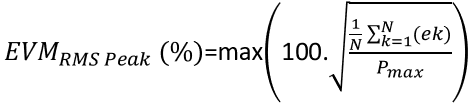
| EVM PeakRMS | Root-Mean-Square of the Error vector magnitude Normalized on Peak Power |
 |
x | |
| EVM Peakpeak | Peak value of the Error vector magnitude Normalized on Peak Power |
 |
x | |
| MER RMS | Root-Mean-Square of the Modulation Error Ratio |
|
x | |
| MER peak | Peak value of the Modulation Error Ratio |
|
x | |
| PAPR | Peak to Average Power Ratio | Max(Pout (dBm))-Mean(Pout (dBm)) | x | |
| Praw (dBm) | Power applied to RF source | Measured by the instrument | x | |
| Pin available (dBm) | Total power available from the drive sources at the DUT plane | Measured by the instrument | x | |
| Pin available PEAK (dBm) | Peak power available from the drive sources at the DUT plane | Pin available AVG (dBm) + PAPRreference(dB) | x | |
| P in delivered (dBm) | Total power delivered to the DUT at the DUT input plane | Measured by the instrument | x(2) | |
| Pout (dBm) | Total power delivered to the load at the DUT output plane. | Measured by the instrument | x | |
| Pout PEAK (dBm) | Peak power delivered to the load at the DUT output plane. | Pout AVG (dBm) + PAPRout(dB) | x | |
| Pdc (dBm) | Total DC power consumed by the DUT | Default : (Vin.Iin)+(Vout.Iout) Could be modified see Consumed Power Expression | x | |
| Pdiss (dBm) | Total power dissipated by the DUT | 10*log10((Pdc(W) +P in delivered(W))-P out (W))+30 | x(2) | |
| Gt (dB) | Transducer gain from the DUT input plane to the DUT output plane | 10.log(Pout (W)/ Pin_available (W)) | x | |
| Gt PEAK (dB) | Transducer gain PEAK from the DUT input plane to the DUT output plane | 10.log(Pout PEAK (W)/ Pin_available PEAK (W)) | x | |
| Gp (dB) | Power gain from the DUT input plane to the DUT output plane | 10.log(Pout(W)/ Pin_delivered (W)) | x(2) | |
| Gt Compression (Max) (dB) | Compression transducer gain refer to the linear gain | Gt max value-Gt measured | x | |
| Gt PEAK Compression (Max) (dB) | Compression transducer gain PEAK refer to the linear gain | Gt PEAK max value-Gt PEAK measured | x | |
| Gp Compression (Max) (dB) | Compression power gain with respect to the linear gain | Gp max value-Gp measured | x(2) | |
| Gt Compression (Linear) (dB) | Compression transducer gain refer to the maximum gain | Gt linear value-Gt measured | x | |
| Gt PEAK Compression (Linear) (dB) | Compression transducer gain PEAK refer to the maximum gain | Gt PEAK linear value-Gt PEAK measured | x | |
| Gp Compression (Max) (dB) | Compression power gain with respect to the linear gain | Gp max value-Gp measured | x(2) | |
| Transducer (%) Efficiency | Transducer Efficiency, efficiency calculated using “Pin_available” | (Pout (W)- Pin_available (W))/ Pdc (W) *100 | x | |
| Drain Efficiency (%) | Drain Efficiency is the efficiency on the output side | Pout (W) / Pdc (W) *100 | x | |
| PAE (%) | PAE, efficiency calculated using “Pin_delivered” | (Pout (W)- Pin_delivered (W))/ Pdc (W) *100 | x(2) | |
| Input Return Loss | Input return loss between the DUT and the source impedance Zsource | 10*log10(Preflect(W)/Pin_available(W))+30 | x(2) | |
| Tmonitor (°C) | Temperature measure by monitor from Thermal Station | Measured by the instrument | x | |
| Tsensor n (°C) | Temperature measure by sensor n from Thermal Station | Measured by the instrument | x | |
| Psensor n (Pa) | Pressure measure by sensor n from Thermal Station | Measured by the instrument | x | |
| Ppm n (dBm) | Power level measure by power meter n from Power Meter Matrix | Measured by the instrument | x |
(2) using three power sensors
| Name | Description | Formula | Level | Reference Waveform | Measured Waveform | DPD Waveform |
|---|---|---|---|---|---|---|
| Index | Index values | All | x | x | x | |
| Time (s) | Waveform duration | Measured by the instrument | I/Q; EVM | x | x | x |
| I (V) | I values | Measured by the instrument | I/Q | x | x | x |
| Q (V) | Q values | Measured by the instrument | I/Q | x | x | x |
| Abs(envelope) (V) | Abs(envelope) | √i2+q2 | I/Q | x | x | x |
| Phase(envelope) (°) | Phase(envelope) | atan2(i,q) | I/Q | x | x | x |
| Mag(envelope) (dBm) | Magnitude(envelope) | 10log10(i2+q2) | I/Q | x | ||
| Constellation | Reference constellation values (only unique values) (1) | Computed using waveform information | Constellation | x | ||
| Demodulated constellation (1) | Measured I/Q demodulated | Computed based on measured waveform using reference waveform information | Constellation | x | x | |
| Normalized frequency (GHz) | Frequency values | -(sampling rate / 2.0) to (sampling rate / 2.0) | Spectrum | x | x | x |
| Raw power (dBm) | Raw power levels | Spectrum | x | x | x | |
| Normalized raw power (dBm) | Raw power levels normalized to 0 | Spectrum | x | x | x | |
| PAP (dB) | Peak to Average Power | Linear step (0 to PAPR maximum) | CCDF | x | x | x |
| Probability (%) | Probability values | 10log10(env(PAPR) - env(mean(PAPR)) | CCDF | x | x | x |
| Pin Available (dBm) | I/Q values corrected by measure Pin Available power | AM/AM; AM/PM | x | x | ||
| Pout (dBm) | I/Q values corrected by measure Pout power | AM/AM; AM/PM | x | x | ||
| AM/AM (dB) | Instantaneous gain conversion | AM/AM | x | x | ||
| AM/PM (°) | Instantaneous phase conversion | AM/PM | x | x | ||
| Symbol (1) | Symbol values | Measured by the instrument | EVM | x | x | x |
| EVM Average [On Signal] | EVM RMS sample per sample in function of time | EVM | x | x | x | |
| EVM Peak [On Signal] | EVM Peak sample per sample in function of time | EVM | x | x | x | |
| EVM Average [On Symbol Carrier n] (1) | EVM RMS symbol per symbol in function of time (n = 1 to 10) | EVM | x | x | x | |
| EVM Peak [On Symbol Carrier n] (1) | EVM Peak symbol per symbol in function of time (n = 1 to 10) | EVM | x | x | x |
(1) only available if reference waveform is a PSK/QAM/LTE/NR5G
Related Information:
NPR
Refer to NPR Measurements
| Name | Description | Formula | Vectorial | Scalar |
|---|---|---|---|---|
| Index | Index values | x | ||
| Time (s) | Measurement time | x | ||
| Ii (A) | Current at port i | Measured by the instrument | x | |
| Vi (V) | Voltage at port i | Measured by the instrument | x | |
| NPRx Ai (dBc) | Noise Power Ratio, so it's the ratio between carrier and xth notch for incident wave at port i | Px notch(dBm)-Pcarrier(dBm) | x | |
| NPRx Bi (dBc) | Noise Power Ratio, so it's the ratio between carrier and xth notch for reflected wave at port i | Px notch(dBm)-Pcarrier(dBm) | x | |
| ACPRi lower or iupper (dBc) | Adjacent Channel Power Ratio, so it's the ratio between carrier and ith adjacent channel on the lower or upper frequency side | Pi lower or iupper(dBm)-Pcarrier(dBm) | x | |
| Praw (dBm) | Power applied to RF source | Measured by the instrument | x | |
| Pin available (dBm) | Total power available from the drive sources at the DUT plane | Measured by the instrument | x | |
| P in delivered (dBm) | Total power delivered to the DUT at the DUT input plane | Measured by the instrument | x | |
| Pout (dBm) | Total power delivered to the load at the DUT output plane. | Measured by the instrument | x | |
| Pdc (dBm) | Total DC power consumed by the DUT | Default : (Vin.Iin)+(Vout.Iout) Could be modified see Consumed Power Expression | x | |
| Pdiss (dBm) | Total power dissipated by the DUT | 10*log10((Pdc(W) +P in delivered(W))-P out (W))+30 | x | |
| Gt (dB) | Transducer gain from the DUT input plane to the DUT output plane | 10.log(Pout (W)/ Pin_available (W)) | x | |
| Gp (dB) | Power gain from the DUT input plane to the DUT output plane | 10.log(Pout(W)/ Pin_delivered (W)) | x | |
| Gt Compression (Max) (dB) | Compression transducer gain refer to the linear gain | Gt max value-Gt measured | x | |
| Gp Compression (Max) (dB) | Compression power gain with respect to the linear gain | Gp max value-Gp measured | x | |
| Gt Compression (Linear) (dB) | Compression transducer gain refer to the maximum gain | Gt linear value-Gt measured | x | |
| Gp Compression (Max) (dB) | Compression power gain with respect to the linear gain | Gp max value-Gp measured | x | |
| Transducer (%) Efficiency | Transducer Efficiency, efficiency calculated using “Pin_available” | (Pout (W)- Pin_available (W))/ Pdc (W) *100 | x | |
| Drain Efficiency (%) | Drain Efficiency is the efficiency on the output side | Pout (W) / Pdc (W) *100 | x | |
| PAE (%) | PAE, efficiency calculated using “Pin_delivered” | (Pout (W)- Pin_delivered (W))/ Pdc (W) *100 | x | |
| Gamma Load | Reflection coefficient presented at the output DUT reference plane | b2/a2 | x(1) | |
| Gamma Source | Reflection coefficient presented at the input DUT reference plane | 0 | x | |
| Gamma In | Reflection coefficient presented by the input of the DUT | b1/a1 | x | |
| Zload (Ω) | Impedance presented at the output DUT reference plane | Z0.(1+Γload/1-Γload) | x(1) | |
| Zsource (Ω) | Impedance presented at the input DUT reference plane by the source | 50 ohms | x | |
| Zin (Ω) | Impedance presented by the input of the DUT | Z0.(1+Γin/1-Γin) | x | |
| AM/PM (°) | Phase Wave ratio between the device input and output | angle(B2/A1) | x | |
| AM/PM (Normalized) (°) | Normalized phase wave ratio between the maximum and the minimum phase shift | max(AMPM)-min(AMPM) | x | |
| Offset AM/PM | Relative phase wave ratio shifts between the device input and output | (AMPM)-first(AMPM) | x | |
| Input Return Loss | Input return loss between the DUT and the source impedance Zsource | |Γin-Γsource*|/|1-(Γin.Γsource| or 10*log10(Preflect(W)/Pin_available(W))+30 | x | |
| Tmonitor (°C) | Temperature measure by monitor from Thermal Station | Measured by the instrument | x | |
| Tsensor n (°C) | Temperature measure by sensor n from Thermal Station | Measured by the instrument | x | |
| Psensor n (Pa) | Pressure measure by sensor n from Thermal Station | Measured by the instrument | x | |
| Ppm n (dBm) | Power level measure by power meter n from Power Meter Matrix | Measured by the instrument | x |
(1) using Full 2-Ports Calibration
| Name | Description | Formula | Level |
|---|---|---|---|
| Index | Index values | All | |
| Normalized frequency (GHz) | Frequency values | -(span / 2.0) to (span / 2.0) | All |
| Spectrum A1 | Available A1 spectrum | Measured by the instrument | A1 |
| Spectrum B1 | Available B1 spectrum | Measured by the instrument | B1 |
| Spectrum A2 | Available A2 spectrum | Measured by the instrument | A2 |
| Spectrum B2 | Available B2 spectrum | Measured by the instrument | B2 |