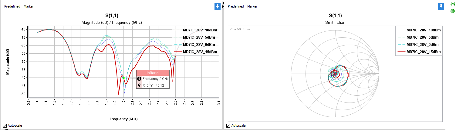
RF and Microwave circuits and instruments are designed with a standard characteristic impedance that is, in most cases, 50 Ohms. The input matching circuit converts the device’s input impedance to the 50-Ohm source impedance and the same for the output, where the matching circuit converts the output impedance to a 50-Ohm load impedance. By designing these matching circuits, we ensure a total power transfer and eliminate reflections. As most instruments, circuits and components are meant to work over a broad frequency bandwidth, it becomes very difficult to guarantee the matching conditions.
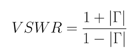
The reflection coefficient can be expressed in a Voltage Standing Wave Ratio (VSWR), representing the impedance mismatch between the output impedance of the power amplifier and the attached load. In some cases, this load is either another circuit or an antenna.

A Power Amplifier designer must ask what level of power reflection can harm the circuit. Or, what is the maximum VSWR that can be presented to the device under test before it is damaged?
To answer this question, test engineers must present to the Power Amplifier different load impedances and conduct power sweeps to reach the operating point or desired compression. Different parameters like Gain, PAE, and power are calculated and plotted on impedance contours to highlight the degradation of these figures of merits with respect to the load impedance presented at the power amplifier’s output.
It is common to perform stress tests where the amplifier is presented at a certain gain compression level with a mismatched load impedance for some time. Then the impedance is changed to 50 Ohm to compare the deterioration of the specifications of the power amplifier caused by long exposure to the mismatch.
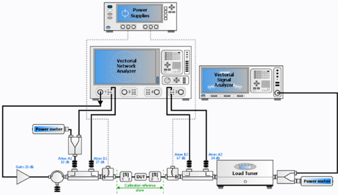
The bench control can be performed using IQSTAR software and the add-on module IQS100B-22. It controls the impedance tuner and synthesizes desired VSWR pattern. The nested sweep of Frequency, power and impedances accelerates the measurement process and provides test engineers with all the necessary data to specify the VSWR conditions of the measured power amplifier.
Spurious emissions measurements
Spurious emissions are undesired radio frequency emissions outside the transmission’s frequency band. These emissions can interfere with other radio services and compromise the intended transmission’s quality.
Many factors can contribute to spurious emissions in a power amplifier. When the power amplifier operates in deep compression, the harmonic content of the output signal can generate spurious emissions. Parasitic oscillations can also cause spurious emissions when the amplifier circuit resonates at a frequency other than the carrier frequency. Another factor that contributes to spurious emissions is crosstalk. Indeed, when the signal on one trace of the power amplifier circuit is coupled to another, it results in spurious emissions.
The spurious emissions can be critical as they can interfere with other signals or channels and reduce the quality of the transmitted signal. Therefore, test engineers must qualify for the quality of the output signal when characterizing power amplifiers and ensure that the spurious level is below the limit set by the regulator.
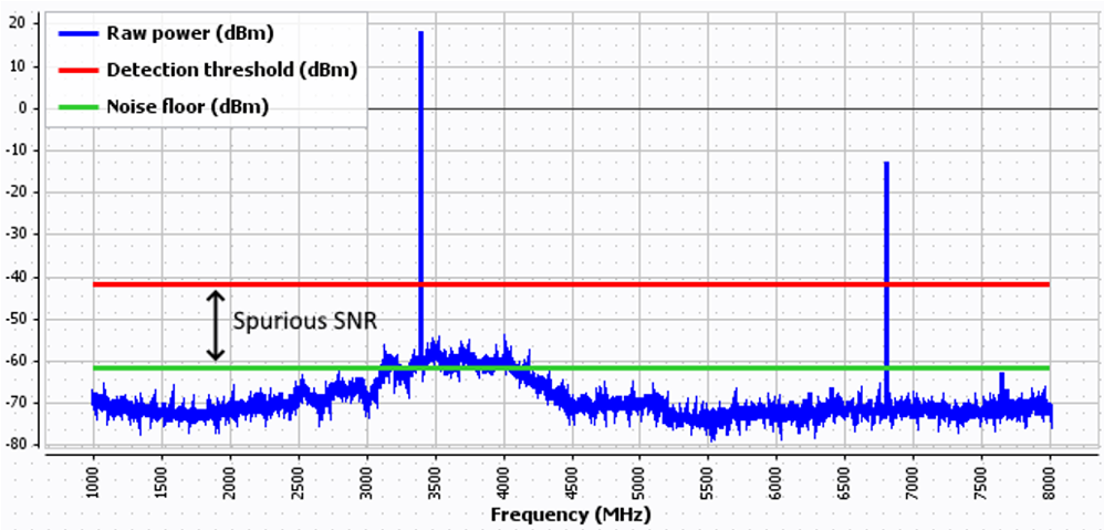
The level of spurious to be detected in the aerospace and defense industries is very low. Therefore, the measurements must be done with a low-resolution bandwidth, considerably slowing the measurement, even with recent fast spectrum analyzers. Furthermore, the spurious emissions must be measured at different bias, frequency, power and load impedance conditions. The measurements can take hours and even days in some cases.
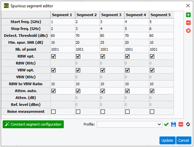
IQS100B-25 uses a fast detection technique based on FFT filters to detect spurs and optimize the measurement time. Multiple settings are possible to adjust the detection level depending on the analyzed bandwidth.