Why do we need a Compact Model?
Compact modeling is the development of integrated semiconductor models for circuit simulations. IC designers are constantly looking for the right model that replicates the terminal behaviours of the device under test (DUT) with precision and yet be simple enough for their circuit simulations. Many semiconductors technology engineers consider physics-based compact models the most accurate, as they can be used for the largest operating range.
However, as their name suggests, they are based on the physics of the device technology and are dedicated to the transistor itself and not to the overall circuit. The nature of the model and the complexity of the equations that need to be solved make it less efficient for circuit-level simulators from the computational standpoint. Therefore, the development of an accurate time efficient equations-based compact model continues to interest many foundries and Fabless design centers due to the increased circuit operating frequencies and the constraining tolerances requested by their customers.
Compact transistor models are based on quasi-isothermal Pulsed IV, Pulsed S-parameters measurement data and Load Pull characterization for model validation. The compact model takes into account complex phenomena like electro-thermal and trapping effects for simulation capabilities under modulated signal conditions.
Compact modelling is the most important step in the circuit design process. It is the key to a first-pass design, time to market and the easiest way to share the information between the transistor manufacturer and the circuit designers.
How to extract a transistor compact model?
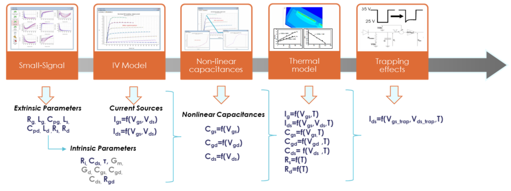
The Compact Model extraction flow of a GaN FET must follow specific guidelines to build a simple -thus computationally efficient- yet complete set of parameters that accurately describe the transistor behaviour, including different complex phenomena like those described above. The flow is sequential and incremental so that different effects are added thanks to dedicated measurement data performed in specific bias conditions (both DC and pulsed), and with appropriate measurement setup.
Measurement Setup
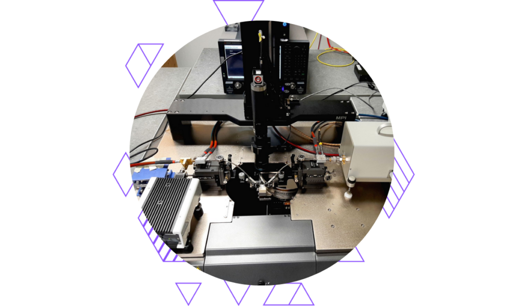
Based on the measurement data, the compact model will only be accurate if we pay particular attention to the quality of the setup by choosing the right instruments, adequate settings, and the right components. On top of that, a precise calibration at the DUT reference plane must be achieved.
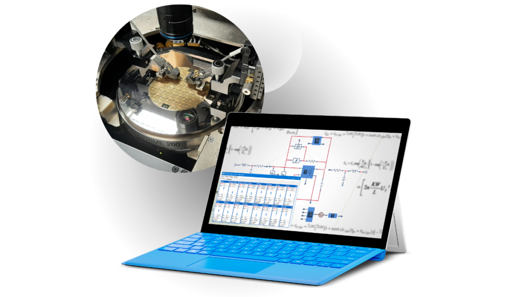
IVCAD MT930J and MT930K associated with the AM3200 Pulsed IV system and Vector Network Analyzer ensure proper synchronization between the instruments and performs accurate and stable Pulsed I-V measurements.
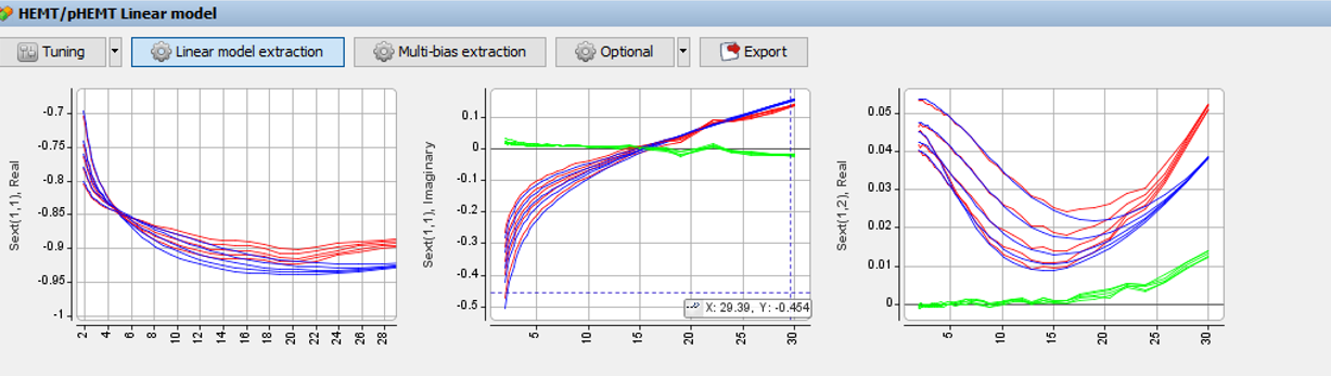
Linear Model Extraction
The extrinsic parameters extraction is the first step of the compact model. The parasitic elements (Rg, Lg, Cpg, Rd, Ld, Cpd, Rs and Ls) are extracted from the S-parameters measurements, which are then de-embedded to the Intrinsic reference plane to extract another set of parameters called Intrinsic parameters (Cgs, Cgd, Gm, Gd, Cds, Ri, Tau, Rgd)
Using IVCAD MT930M1, a step-by-step process offers the modelling engineer a powerful yet easy tool to extract the associated linear parameters. During the optimization process, measured and modelled S-parameters are compared at the intrinsic and extrinsic reference planes.
Nonlinear Model Extraction
Pulsed I-V networks measured using the AM3200 help extract the nonlinear Model parameters. Measurements are done in different conditions of quiescent levels, chuck temperatures, pulse widths and drain voltages sweeps are used to study the thermal effects on the performances, including self-heating, in safe operating regions and to study the breakdown region of the transistor. Quasi iso-thermal conditions are obtained using short pulse widths to avoid strong temperature variation during the pulse, and small duty-cycles keep a low averaged variation of the temperature during the whole pulse period.

Starting from the iso-thermal model, different phenomena are then added one after the other to understand and correctly describe the effect of each of them independently from one another.
Trapping Effects
Trapping effects are parasitic effects resulting from impurities or defects in the crystalline network of the transistor material that reduces the maximum output current. Indeed, the charging and discharging of the traps have a direct effect on Ids creating current collapses.
With the help of the AM3200 Pulsed IV system and its capabilities to allow the selection of different quiescent levels, we can study the effect of the surface trapping (Gate-Lag) and buffer trapping (Drain-Lag)
The trapping phenomena are included in the compact model to ensure a proper prediction of the current source behaviour during large signal application of the transistor.
Load Pull Characterization for Model Validation
Load Pull characterization is used to validate compact models in application-like conditions. As the model is supposed to predict the transistor’s behaviour in a condition beyond 50Ω load termination, measurements are done with a load pull setup and IVCAD MT930C at the intrinsic reference plane, using the extrinsic Netlist to de-embed the measurement.
Vector receiver load pull with time domain capabilities (MT930GA) can measure the dynamic load line and compare it to the modelled result. This methodology enables validation and the possibility of tuning the compact model for a better agreement between measurements and the model for a specific application.
