Why do we need to characterize RF devices using Pulsed I-V and RF Measurements?
Transistor characterization is an important step in any large signal nonlinear circuit design. Be it a Power amplifier, a switch or an LNA, the characteristics of the transistor used to design an RF and Microwave circuit need to be well known. Nonlinear RF circuit designs are based on transistors models provided by the foundries. The better the model predicts the behaviour of the transistor, the closest the design is to the real circuit. Pulsed current-voltage (I-V) and Pulsed S-Parameters measurements are invaluable techniques for assessing the performances of semiconductor devices.
The pulsed I-V measurements ensure Quasi-isothermal conditions, avoiding the negative effects of self-heating and minimizing transient trapped charges. Using short pulses and/or low duty cycle periods maintains the DUT performances during the measurements, which is impossible with DC bias. These measurements are done using a pulsed I-V system and a Vector Network Analyzer for the S-Parameters.
How do we perform pulsed I-V measurements?
Pulsed I-V measurements are performed using pulsed sources to stimulate the transistor under test and a pulse measurement system. The typical measurements are Pulsed I-V sweeps and time-domain voltage and current acquisitions.
The device under test (DUT) is connected to the power supplies through bias tees. These later need to be chosen carefully to support these measurements. On the one hand, they need to support the voltage and current specifications of the transistor. On the other hand, the bias circuit needs to have a bandwidth large enough to handle pulsed biasing signals. The RF ports of the bias tees should be terminated with 50Ohm loads to avoid transistor oscillations.
Using an AM3200 Pulsed I-V system from AMCAD Engineering, one can produce curves showing the drain voltage versus the drain current variation for different gate voltage conditions.
The gate pulser AM3211 is connected to the bias tee at the input of the DUT, and the AM3221 module is connected to the bias tee at the output. Most pulsed I-V measurements for Device Characterization or model extraction purposes are done at the die level, but it is always possible to perform these measurements on a packaged device.

Pulsed I-V Measurements for RF and microwave devices
Multiple phenomena impact transistor behaviour. The PIV system should be able to capture these behaviours while ensuring a safe operation of the transistor to avoid failures.
The Pulse swing should be controllable. one level of the pulse is called Quiescent, or operating point and the other level is called peak level or Non-Quiescent level. A Pulsed I-V system should be able to set the Quiescent and the Peak level to any values. The Duty cycle is also a very important measurement condition. It relates to the ratio between the duration of the peak level over the total pulse period in %.
I-V Network is measured by sweeping the output voltage for different input voltage values. These measurements highlight the nonlinear characteristics of the DUT and help understand its behaviour when a large signal is applied. Each measurement point of the network represents a voltage and current acquisition during a portion of the pulse where the signal is settled or flat. Usually, these measurements are averaged over many pulses to increase the accuracy of the measurement results. The breakdown voltage is also possible to obtain, but with extra caution as we tend to reach the breaking point of the device. The self-heating and temperature dependency of the measured current imposes certain conditions to understand these behaviours. The Pulse width and duty cycle of the bias conditions allow quasi-isothermal measurements to have a reference compared to high junction temperature conditions. The choice of the quiescent bias point is also important in controlling the gate lag and drain lag of GaN-based devices.
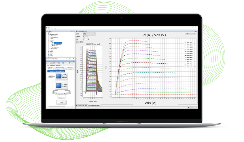
Transient I-V measurements allow designers to capture ultra-high-speed current or voltage waveforms in the time domain to study dynamic properties.
The results are displayed as the pulse shape versus time averaged over multiple pulses capturing any time-varying changes, like the effects of self-heating or charge trapping.
Using the AM3200 from AMCAD, the MT930J option of IVCAD allows complete control of the instrument to measure Pulsed I-V networks, time domain waveforms of the voltage and current, breakdown voltage, and long pulse response for up to 200s pulse period.
MT930E option is a subset of the MT930J where the user can measure I-V networks in DC mode using regular DC Power Supplies
Pulsed S-Parameters Measurements
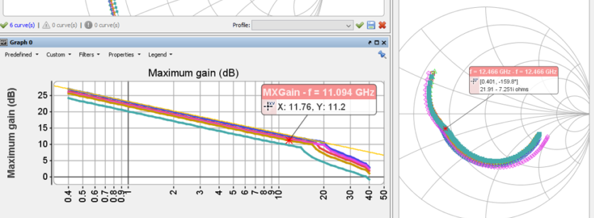
A full characterization of an RF transistor includes small and large signal testings. The small signal testing is performed using a Vector network analyzer to measure the S-parameters at the RF ports of the DUT. This measurement requires a rigorous calibration process to shift the reference plane as close to the DUT as possible. Although the S-Parameters are commonly measured in CW mode, it requires more attention when measured in Pulsed mode.
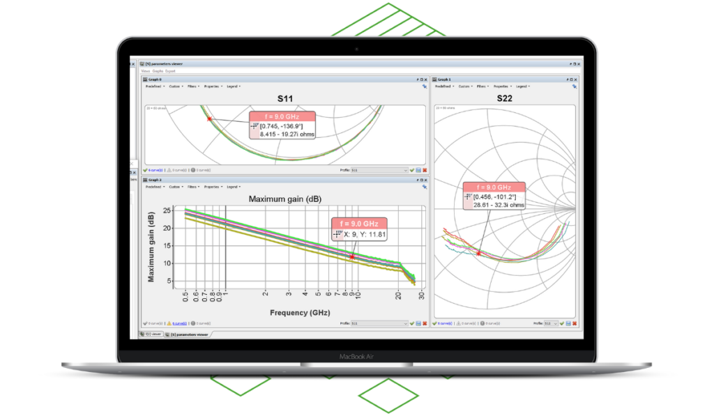
VNAs need to have all required pulsed options for the generation, the measurements and the triggering. The signal timing needs to be well synchronized with the pulsed voltage to ensure a proper biasing of the DUT. The RF signal measurements are controlled by a gated window where the pulse shape is as flat as possible, avoiding transient mode.
MT930K option of IVCAD ensures proper synchronization of the VNA with the Pulsed I-V system for accurate and stable S-parameters measurements. The module includes all necessary settings to choose between the triggering options and data acquisition modes depending on the available instruments and pulse options.
MT930F is a subset of the MT930K option where the user can only measure S-parameters in CW mode.
